
Title here
Summary here
The example designs for the Ethernet FMC are hosted on Github. There are currently six designs, hosted in separate repositories. Each example design supports multiple development boards and they all work with the Ethernet FMC and the Robust Ethernet FMC interchangeably.
| Example Designs | |||
|---|---|---|---|
| AXI Ethernet Example Design | More info | Git repo | Docs |
| PS GEM Example Design | More info | Git repo | Docs |
| Open-source MAC (Taxi) Example Design | More info | Git repo | Docs |
| Maximum Throughput Example Design | More info | Git repo | Docs |
| Network Tap Example Design | More info | Git repo | Docs |
| Processorless Example Design | More info | Git repo | Docs |
This example design is based on AMD’s soft MAC (ie. FPGA implemented), the AMD Xilinx AXI 1G/2.5G Ethernet Subsystem IP , that can be found in the Vivado IP Catalog. As the MAC is implemented in the FPGA fabric, this example is ideal for pure FPGA designs or Zynq/ZynqMP designs that require some packet processing to be performed in the FPGA. Each of the four ports has its own AXI Ethernet Subsystem and AXI DMA. The design comes with an lwIP echo server bare-metal application and a Linux (PetaLinux/Yocto) flow, and it targets MicroBlaze, Zynq-7000, Zynq UltraScale+ and Versal development boards.

This example design utilizes the Gigabit Ethernet MACs (GEMs) that are embedded into the Processing System (PS) of the Zynq 7000 and Zynq Ultrascale+ devices. The embedded MACs used in this example design do not use up any of the FPGA fabric, which makes it ideal for applications that need to use the FPGA for other purposes.
The Zynq 7000 based designs use one of the embedded MACs (GEMs) and three AXI Ethernet Subsystem IP blocks to implement all 4 ports of the Ethernet FMC.

The Zynq Ultrascale+ based designs use all four of the GEMs to implement the ports of the Ethernet FMC.

This example design drives the four gigabit ports with a fully open-source Ethernet MAC. Each port uses a 1G RGMII MAC from the FPGA Ninja Taxi transport library paired with an AMD AXI DMA. There is no AXI Ethernet Subsystem in the design, so no separately licensed AMD IP is needed to build it, and the source of the MAC is in the repository for you to read, simulate and modify. The design runs an lwIP echo server on all four ports (bare-metal) and has a Yocto Linux flow with a netdev driver for the Zynq UltraScale+ target. The MicroBlaze target is standalone only and is loaded over JTAG.

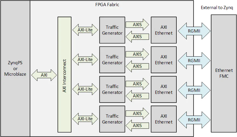
This example design demonstrates the use of an FPGA based packet generator designed in HLS to achieve raw data transmission over the Ethernet ports at the maximum throughput. The packet generator IPs drive the AXI Ethernet Subsystem IPs with a continuous stream of packets, as well as checking the received packets for bit errors. The software application polls the MACs to detect any dropped packets. The design targets the ZedBoard Zynq-7000 Development board .
As a packet based network technology, Ethernet links have overheads which prevent them from being exploited at 100% channel efficiency. We can however get close to 100% channel efficiency by sending packets with the largest acceptable payload and by operating on the lowest protocol layer – this is what we do to measure the maximum throughput of the Ethernet FMC.
The maximum throughput design uses a hardware packet generator, to continuously feed Ethernet packets to the AXI Ethernet Subsystem (ie. the MAC). The packet generator is configured by the CPU through several software registers for parameters such as payload size and inter-packet delay. The generated packets are standard Ethernet frames which are composed of destination/source MAC addresses, an EtherType or length code, a payload and a checksum. The payload is generated by a 32-bit linear feedback shift register (LFSR) to produce randomly varying content that can be easily verified by the receiver.
The table below shows our measurements of maximum effective throughput per port which were performed at various payload sizes. They serve as a performance benchmark for the Ethernet FMC in designs with no bottlenecks in the data path to the MAC. The results also demonstrate the relationship between payload size and channel efficiency.
The measurements were made by using a debug probe on the AXI-Streaming interface of the Tri-mode Ethernet MACs while all four ports of the Ethernet FMC were transmitting and receiving simultaneously.
Note that these tests only demonstrate the possible throughput when using standard Ethernet frames. It would however be possible to achieve even higher throughput by using non-standard jumbo frames.
| Payload size (bytes) | Effective throughput (Mbps) | Channel efficiency |
|---|---|---|
| 66 | 652 | 65.19% |
| 438 | 915 | 91.49% |
| 810 | 946 | 94.60% |
| 1182 | 969 | 96.89% |
| 1498 | 974 | 97.35% |
This example design turns the Ethernet FMC into a hackable, passive in-line network tap. Two of the Ethernet ports are bridged in the FPGA fabric so that traffic passes straight through between them, while everything that passes is mirrored out of a third port for monitoring or capture. The bridged path is implemented with GMII-to-RGMII converters and FIFOs in the fabric, and the mirror port runs an lwIP application on the processor. It is intended as a starting point for your own packet inspection, filtering or logging logic.

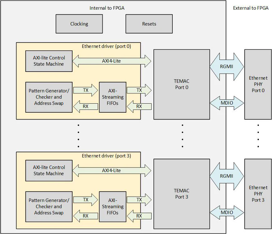
This example demonstrates how the Ethernet FMC can be used without a processor. All of the packet generation and processing is done entirely by state machines in the FPGA fabric. The design also contains the logic for bringing up the PHYs and configuring the TEMAC. It is bitstream-only and runs a hardware traffic loopback on all four ports, which makes it a good way to prove the FMC on FPGA boards that have no processor and no transceivers.
You can read more about the processorless design in this three part blog: